

Sequential Circuits: Exploring Memory, Timing, and Counters
Exploring the Mechanisms of Flip-Flops, Latches, and Counters in Digital Systems

In sequential logic the output of the logic device is dependent not only on the present inputs to the device, but also on past inputs; i.e., the output of a sequential logic device depends on its present internal state and the present inputs. This implies that a sequential logic device has some kind of memory of at least part of its “history” (i.e., its previous inputs). Sequential circuits include storage elements like flip-flops, which store information, or state, and allow the circuit to exhibit memory.
In simple words sequential circuits are just combinational circuits with memory.

They can be represented by a feedback model, capacitive model or implicit model.
1. Feedback Model
The feedback model is a fundamental concept in sequential circuits where the output of a circuit is fed back into its input. This feedback creates a loop, allowing the circuit to "remember" its previous state, thereby making it possible for the circuit to exhibit memory or state-dependent behavior. The feedback model is commonly used in the design of latches and flip-flops, which are the basic building blocks of sequential circuits.
Positive Feedback: In this case, the feedback reinforces the current state, stabilizing the circuit in one of its possible states. For example, in a bistable latch, positive feedback ensures that the circuit remains in one of two stable states until an external input forces a change.
Negative Feedback: Here, the feedback works to stabilize the circuit by opposing changes in the output. Negative feedback is more common in analog circuits, such as amplifiers, but in digital circuits, it can help improve stability and reduce the effects of noise.
2. Capacitive Model
The capacitive model is typically used to describe the behavior of dynamic circuits, especially in the context of charge storage and transfer. In digital circuits, capacitance plays a crucial role in the operation of devices like dynamic RAM (DRAM) and charge-coupled devices (CCDs).
Charge Storage: In such a model, the capacitor is used to store charge, representing a binary value (e.g., 0 or 1). The stored charge on the capacitor determines the state of the circuit.
Dynamic Operation: Unlike static storage elements (like flip-flops), which maintain their state indefinitely as long as power is supplied, capacitive storage elements need to be periodically refreshed because they lose their charge over time due to leakage currents. This dynamic nature makes capacitive circuits faster but also more complex, as they require refresh mechanisms.
3. Implicit Model
The implicit model in sequential circuits refers to the indirect or hidden way in which timing and state dependencies are handled within the circuit design. Rather than explicitly defining the timing relationships, the implicit model relies on the natural propagation delays and inherent circuit properties to ensure correct operation.
Timing and Propagation Delays: In the implicit model, the design assumes that certain operations will complete within expected time frames due to the natural propagation delays through the circuit elements. This model is often used in asynchronous circuit design, where there is no global clock signal to synchronize operations.
Race Conditions and Hazards: Because the implicit model does not explicitly control timing, it is more susceptible to race conditions and hazards, where different parts of the circuit may incorrectly process signals if the timing assumptions are violated. Careful design and analysis are required to ensure that the circuit operates reliably under the implicit model.
Types of Sequential circuits:
There are 2 types of sequential circuits
1)Synchronous Sequential Circuits
Synchronous sequential circuits are those where changes in the state of the circuit occur in synchrony with a clock signal. This clock signal acts as a timing reference for all state transitions within the circuit. The operation of these circuits depends on clock pulses, which help in coordinating the activities of various parts of the system.These include flip flops and finite state machines.
a)Flip-Flops
Flip-flops are the basic building blocks of synchronous sequential circuits. They are bistable devices, meaning they have two stable states (0 and 1) and can store one bit of data. Flip-flops are edge-triggered, meaning they change state only at the edge of the clock signal (either rising edge or falling edge).
Types of Flip-Flops:
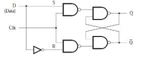
SR Flip-Flop (Set-Reset Flip-Flop):
Inputs: Set (S), Reset (R), Clock (CLK)
The SR flip-flop sets or resets the output Q based on the S and R inputs. If S = 1 and R = 0, Q is set to 1. If S = 0 and R = 1, Q is reset to 0. If both S and R are 0, Q retains its previous state. The case where both S and R are 1 simultaneously is typically avoided because it leads to an indeterminate state.
D Flip-Flop (Data Flip-Flop):
Inputs: Data (D), Clock (CLK)
The D flip-flop transfers the D input to the Q output on the edge of the clock signal. It ensures that the output follows the input at the clock edge, making it a simple and widely used flip-flop.
JK Flip-Flop:
Inputs: J, K, Clock (CLK)
The JK flip-flop is a refinement of the SR flip-flop that eliminates the indeterminate state. If J = 1 and K = 0, Q is set to 1. If J = 0 and K = 1, Q is reset to 0. If J = K = 1, the output toggles (i.e., switches to the opposite state).
T Flip-Flop (Toggle Flip-Flop):
Inputs: Toggle (T), Clock (CLK)
The T flip-flop toggles its state on each clock edge if T = 1. If T = 0, the output remains unchanged. The T flip-flop is often used in counters.
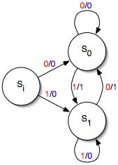
Finite State Machines (FSMs)
Finite State Machines (FSMs) are a model of computation used to design sequential circuits. An FSM consists of a finite number of states, transitions between these states, and actions that occur in response to events.
Moore Machine: In a Moore machine, the output depends only on the current state, not on the input. The output is a function of the state itself.

Mealy Machine: In a Mealy machine, the output depends on both the current state and the input. This allows Mealy machines to react faster to inputs, as the output can change immediately when an input changes.

Asynchronous Sequential Circuits
Asynchronous sequential circuits do not rely on a clock signal to synchronize their operations. Instead, changes in the circuit's state occur in response to changes in the input signals. These circuits are more complex to design and analyze due to potential timing issues like race conditions and hazards.
Latches
Latches are the basic memory elements used in asynchronous sequential circuits. Unlike flip-flops, latches are level-sensitive rather than edge-triggered, meaning they respond to changes in input levels rather than clock edges. They are actually single bit storage elements.
Types of Latches:
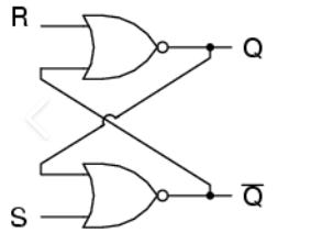
SR Latch (Set-Reset Latch):
Inputs: Set (S), Reset (R)
It ties set and reset inputs and have cross coupled NAND/NOR gates
Data is stored at Q.
S and R are control inputs.
Both inputs are high at ideal state
S=0 and R=1 to change Q to Q=1 (Set)
R=0 and S=1 to change Q to Q=0 (Reset)
See verilog implentation SR Latch


D Latch:
Inputs: Data (D), Enable (EN)
The D latch is a transparent latch, meaning it passes the input D to the output Q when the enable signal is active. When the enable signal is inactive, the output remains unchanged.

JK Latch:
Inputs: J, K
: Just like SR latch it eleminates undefined state of SR Latch
T Latch:
Inputs: Toggle (T)
If we short JK inputs we get T latch. In this outputs are toggled when inputs are high

Low Active and High Active Signals
Digital circuits often use signals that are either low-active or high-active, depending on the logic level that triggers their action.
Low-Active Signals: These signals perform their action when the input is at a low logic level (0). For example, a low-active reset signal will reset the circuit when the reset input is 0.
High-Active Signals: These signals perform their action when the input is at a high logic level (1). A high-active reset signal will reset the circuit when the reset input is 1.
Applications of Sequential circuits
Counters
These circuits count the number of clock pulses and are used in timing applications.They are essentially a sequential circuit that goes through a predefined sequence of states, typically representing a numerical count. Counters are widely used in applications like digital clocks, event counters, frequency dividers, and in various timing and control circuits.
Types of Counters:
1. Asynchronous Counters (Ripple Counters)
Asynchronous counters, also known as ripple counters, are the simplest type of counters where the clock input is applied to the first flip-flop, and the output of each flip-flop serves as the clock input for the subsequent flip-flop.
Explanation
The first flip-flop toggles its state with each incoming clock pulse.
The change in state of the first flip-flop triggers the second flip-flop, and this ripple effect continues through the entire chain of flip-flops.
This cascading effect creates a delay, as each flip-flop waits for the previous one to toggle before it can change its state.
Propagation Delay: The ripple effect causes a delay in the output, making asynchronous counters slower compared to synchronous ones.
Simple Design: The design is straightforward since each flip-flop is only concerned with the output of the preceding one.
Example:
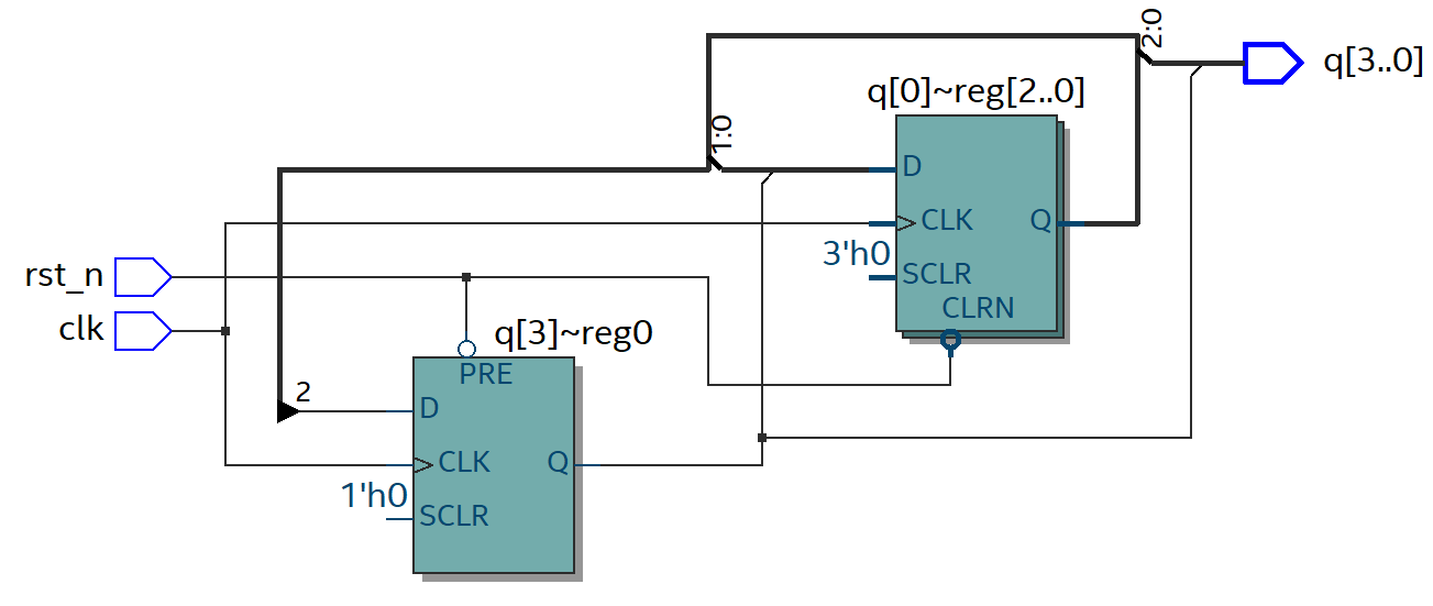
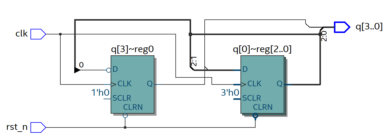
A 3-bit asynchronous counter counts from 000 to 111 (0 to 7 in decimal). When the first flip-flop toggles from 0 to 1, it causes the second flip-flop to toggle, and so on.
2. Synchronous Counters
In synchronous counters, all flip-flops receive the clock signal simultaneously, eliminating the ripple effect seen in asynchronous counters. This design allows for faster operation and more reliable timing.
Explanation:
The clock signal is directly applied to all flip-flops in the counter.
A common control logic is used to determine when each flip-flop should toggle, ensuring that all flip-flops change state in sync with the clock.
Simultaneous Toggling: All flip-flops toggle simultaneously in response to the clock pulse.
Complex Design: Requires additional logic gates to manage the synchronous operation of flip-flops.
Example:
Binary Counter
A binary counter counts in binary, typically from 0 to 2^n - 1, where n is the number of flip-flops.
Each flip-flop represents one bit of the binary count. For example, a 4-bit binary counter counts from 0000 (0) to 1111 (15 in decimal).
Decade Counter
A decade counter is a counter that counts from 0 to 9 and then resets to 0, making it ideal for counting decimal digits.
This counter usually involves additional logic to reset the count after reaching 9 (1001 in binary).
Example Digital Clock
Up Counter
An up counter increments its count with each clock pulse, counting upwards from a minimum value (usually 0) to a maximum value before resetting.
Example: A 3-bit up counter counts from 000 to 111 (0 to 7 in decimal).
Down Counter
A down counter decrements its count with each clock pulse, counting downwards from a maximum value to a minimum value before resetting.
Example: A 3-bit down counter counts from 111 to 000 (7 to 0 in decimal).
Up/Down Counter
An up/down counter can count both upwards and downwards, depending on a control signal.
If the control signal is set to "up," the counter increments; if set to "down," the counter decrements.
Ring Counter
A ring counter is a type of counter where only one flip-flop is set to 1, and all others are set to 0. The "1" bit circulates through the flip-flops, creating a ring-like pattern.
If a ring counter has four flip-flops, it will cycle through the states 1000, 0100, 0010, 0001, and back to 1000.

Johnson Counter (Twisted Ring Counter)
Description: A Johnson counter is similar to a ring counter but with a twist; the output of the last flip-flop is inverted and fed back to the first flip-flop.


Registers
In sequential logic, registers are used to store data across clock cycles, providing a means for the circuit to "remember" previous states. This capability is essential for building circuits that require memory, such as counters, shift registers, and state machines.
Registers operate by capturing and holding data on the arrival of a clock edge (rising or falling). The data stored in the register can then be used in subsequent operations, allowing the circuit to maintain a state across multiple clock cycles.
Types of Registers in Sequential Logic:
D Register (Data Register):
Captures and stores the value of the data input on the clock edge.
The data at the input (D) is transferred to the output (Q) on the clock edge. This type of register is commonly used for simple data storage and transfer tasks.
Example: A D flip-flop-based register.
Shift Register:
Shifts data bits through a series of flip-flops on each clock cycle.
Data is shifted left or right through the register, allowing for operations such as data serialization and parallel-to-serial conversion.
Example: A 4-bit shift register where data can be shifted through four stages.
Counter Register:
Counts clock pulses and stores the count value.
The register increments or decrements its value with each clock pulse, often used in timers, frequency dividers, and event counters.
Example: A 4-bit binary counter that counts from 0 to 15.
Latch Register:
Holds data based on an enable signal rather than a clock edge.
Data is transferred to the output when the enable signal is active, allowing for level-sensitive storage.
Example: An SR latch or D latch used for temporary data storage.
Role in Sequential Circuits:
State Storage: Registers maintain the state of a sequential circuit, enabling it to process data based on both current inputs and past values. This state retention is crucial for implementing complex behaviors like state machines.
Synchronization: Registers synchronize data with a clock signal, ensuring that changes occur in a controlled manner. This synchronization is essential for ensuring that sequential circuits operate correctly and predictably.
Data Transfer: Registers facilitate the transfer of data between different stages of a sequential circuit, enabling modular design and complex processing tasks.
Memory Cells
Memory cells are the smallest units of data storage in a memory system. They hold individual bits of information (0 or 1) and are organized into arrays to form larger memory structures. The design and functionality of memory cells are crucial for the overall performance and efficiency of memory systems.
Types of Memory Cells
1. Static RAM (SRAM) Cells
SRAM cells use flip-flops to store each bit of data. Unlike dynamic RAM (DRAM), SRAM does not need to be periodically refreshed.
Each SRAM cell consists of a set of transistors arranged in a configuration that maintains a stable data state as long as power is supplied.
The flip-flops in SRAM cells provide high-speed access and low latency, making SRAM ideal for cache memory and high-performance applications.
Characteristics:
Speed: Fast access times.
Power Consumption: Higher power consumption compared to DRAM due to the continuous power required to maintain the state.
Size: Larger cell size, resulting in less density compared to DRAM.
Applications:
Used in cache memory, registers, and high-speed buffer storage.
2. Dynamic RAM (DRAM) Cells
DRAM cells use a single transistor and a capacitor to store each bit of data. The capacitor holds the data as a charge, representing a binary value.
The transistor acts as a switch that controls access to the capacitor. When data is read, the charge on the capacitor is measured and then refreshed to restore the charge.
DRAM cells require periodic refreshing to maintain data integrity, as capacitors leak charge over time.
Characteristics:
Speed: Slower access times compared to SRAM.
Power Consumption: Lower power consumption due to the refresh mechanism and simpler cell structure.
Size: Smaller cell size, allowing higher density and more memory capacity.
Applications:
Commonly used in main memory (RAM) for computers, smartphones, and other devices requiring large amounts of data storage.
3. Flash Memory Cells
Flash memory cells are a type of non-volatile memory that retains data even when power is off. Flash memory uses floating-gate transistors to store data.
Data is stored by trapping electrons in a floating gate within a transistor. The presence or absence of electrons represents binary data.
Flash memory cells are organized into blocks and pages, which can be programmed and erased in bulk.
Characteristics:
Speed: Slower write and erase speeds compared to SRAM and DRAM.
Power Consumption: Low power consumption and non-volatile nature make it ideal for portable devices.
Endurance: Limited number of write/erase cycles compared to SRAM and DRAM.
Applications:
Used in USB drives, solid-state drives (SSDs), and memory cards for data storage.
4. EEPROM (Electrically Erasable Programmable Read-Only Memory) Cells
EEPROM cells are non-volatile memory cells that can be electrically erased and reprogrammed.
Similar to flash memory, EEPROM uses floating-gate transistors but allows for byte-level erasing and programming rather than block-level.
Characteristics:
Speed: Generally slower than flash memory for write operations.
Power Consumption: Low power consumption and non-volatile.
Endurance: Higher endurance for write/erase cycles compared to flash memory.
Applications:
Used in applications requiring frequent updates and small amounts of data storage, such as configuration settings in embedded systems
Connect with Me:
LinkedIn: Rana Umar Nadeem
Medium: @ranaumarnadeem
GitHub: ranaumarnadeem/HDL
Substack: We Talk Chips
Tags: #DigitalLogic #CombinationalLogic #Adders #Decoders #Encoders #Mux #Demux #Subtractors #Multipliers #Verilog #HDL #DigitalDesign #FPGA #ComputerEngineering #TechLearning #Electronics #ASIC #RTL #Intel #AMD #Nvidia#substack #github #DFT #DLD #Digital logic#sequential logic #medium #moorelaw #FSM
Amazing 🔥 Great work sir !
This just excites me more about chips and EE